- 您现在的位置:买卖IC网 > Sheet目录409 > DR-TRC101-315-DK (RFM)RFIC TRANCEIVER DEVELOPMENT KIT
�� �
�
�FIFO� and� RESET� Mode� Configuration� Register� [POR=CA80h]�
�Bit�
�15�
�1�
�Bit�
�14�
�1�
�Bit�
�13�
�0�
�Bit�
�12�
�0�
�Bit�
�11�
�1�
�Bit�
�10�
�0�
�Bit�
�9�
�1�
�Bit�
�8�
�0�
�Bit�
�7�
�FINT3�
�Bit�
�6�
�FINT2�
�Bit�
�5�
�FINT1�
�Bit�
�4�
�FINT0�
�Bit�
�3�
�0�
�Bit�
�2�
�FIFST�
�Bit�
�1�
�FILLEN�
�Bit�
�0�
�RSTEN�
�The� Data� FIFO� Configuration� Register� configures:�
�?�
�?�
�?�
�?�
�FIFO� fill� interrupt� condition�
�FIFO� fill� start� condition�
�FIFO� fill� on� synchronous� pattern�
�RESET� Mode�
�Bit� [15..8]� -� Command� Code� :� These� bits� are� the� command� code� that� is� sent� serially� to� the� processor� that�
�identifies� the� bits� to� be� written� to� the� Data� FIFO� Configuration� Register.�
�Bit� [7..4]� –� FIFO� Fill� Bit� Count� :� This� sets� the� number� of� bits� that� are� received� before� generating� an�
�external� interrupt� to� the� host� processor� that� the� receive� FIFO� data� is� ready� to� be� read� out.� It� is� possible� to�
�set� the� maximum� fill� level� to� 15,� but� the� designer� must� account� for� the� processing� time� it� will� take� to� read�
�out� the� data� before� a� register� overrun� occurs,� at� which� data� will� be� lost.� It� is� recommended� to� set� the� fill�
�value� to� half� of� the� desired� number� of� bits� to� be� read� to� ensure� enough� time� for� additional� processing.�
�See� Status� Register� for� description� of� FIFO� status� bits� that� may� be� read� and� FIFO� Read� Register� for�
�polling� and� interrupt-driven� FIFO� reads� from� the� SPI� bus.�
�Bit� [3]� –� Not� Used� .� Write� a� “0”.�
�Bit� [2]� –� FIFO� Fill� Start� Condition� :� This� bit� sets� the� condition� at� which� the� FIFO� begins� filling� with� data.�
�When� set,� the� FIFO� will� continuously� fill� regardless� of� noise� or� good� data.� When� clear,� the� FIFO� will� fill�
�when� it� recognizes� the� synchronous� pattern� as� defined� internally.� The� internal� pattern� is� 2DD4h.�
�Note:� This� pattern� is� not� configurable� and� is� not� accessible� to� a� host� processor.�
�Bit� [1]� –� Synchronous� Pattern� FIFO� Fill� :� When� set,� the� FIFO� will� begin� filling� with� data� when� it� detects�
�the� synchronous� pattern� as� defined� in� Bit� [2].� The� FIFO� fill� stops� when� this� bit� is� cleared.� To� restart� the�
�synchronous� pattern� recognition,� simply� clear� the� bit� and� set� again.�
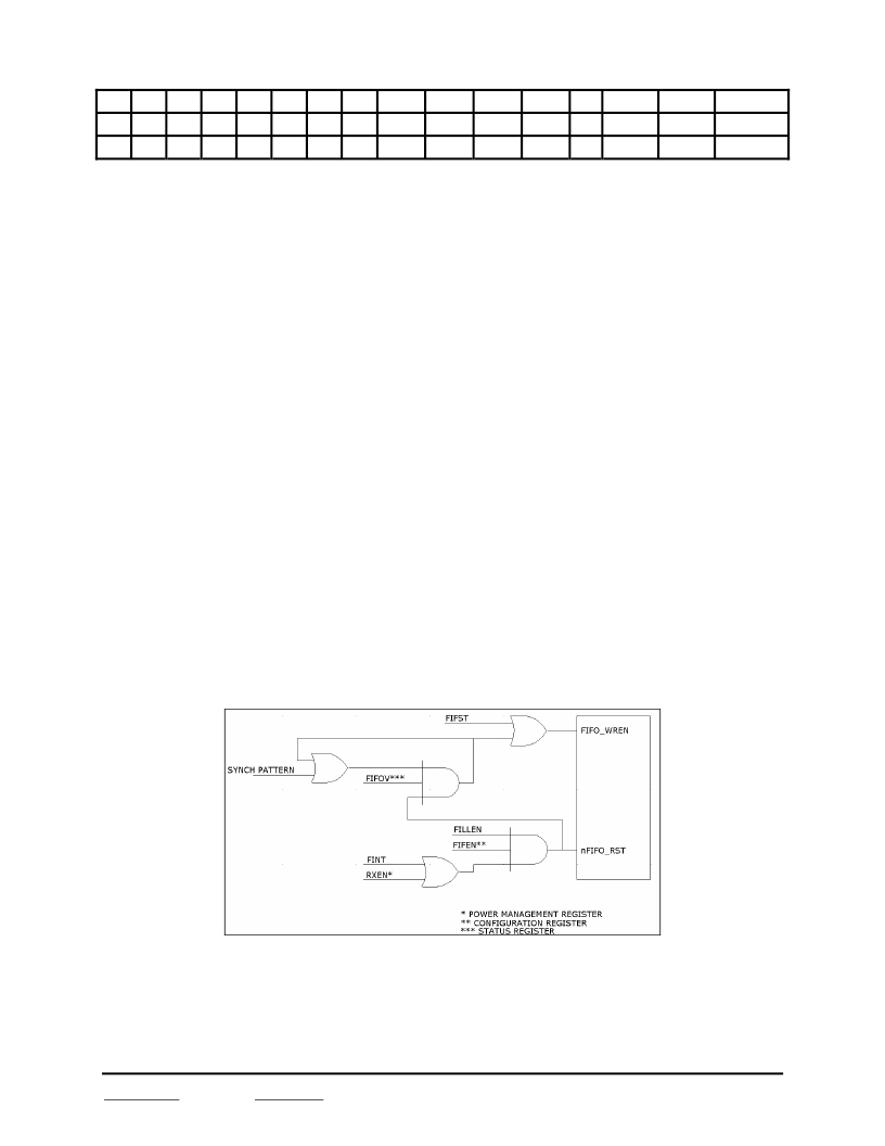
�Note:� Clearing� this� bit� will� issue� a� FIFO� reset.� See� Figure� 9� for� FIFO� write� and� reset�
�configuration.�
�Figure� 9.� FIFO� Write� and� Reset� Configuration�
�Bit� [0]� –� Disable� RESET� Mode� :� When� cleared,� if� the� TRC101� encounters� a� 0.2V� spike� in� the� power�
�supply,� the� glitch� could� cause� a� system� reset.� When� set,� this� mode� is� disabled.�
�www.RFM.com�
�Email:� info@rfm.com�
�Page� 26� of� 42�
�?by� RF� Monolithics,� Inc.�
�TRC101� -� 4/8/08�
�发布紧急采购,3分钟左右您将得到回复。
相关PDF资料
DR-TRC102-915-DK
RFIC TRANCEIVER DEVELOPMENT KIT
DR-TRC103-915-DK
RFIC TRANCEIVER DEVELOPMENT KIT
DR-TRC103-950-DK
KIT DEV 950MHZ RFIC SRR
DR-TRC105-372-DK
DEV KIT TRC105
DR-TRC105-450-EV
BOARD EVALUATION 450MHZ RFM RFIC
DR-TXC100-433
BOARD EVALUATION 433MHZ TXC100
DR-WLS1273L-EV
KIT EVAL FOR WLS1273L
DR7000-DK
3G DEVELOPMENT KIT 433.92MHZ
相关代理商/技术参数
DR-TRC102-433-DK
功能描述:射频开发工具 TRC102 Development Kit 430-439 MHz RoHS:否 制造商:Taiyo Yuden 产品:Wireless Modules 类型:Wireless Audio 工具用于评估:WYSAAVDX7 频率: 工作电源电压:3.4 V to 5.5 V
DR-TRC102-868-DK
功能描述:射频开发工具 TRC102 Development Kit 860-879 MHz RoHS:否 制造商:Taiyo Yuden 产品:Wireless Modules 类型:Wireless Audio 工具用于评估:WYSAAVDX7 频率: 工作电源电压:3.4 V to 5.5 V
DR-TRC102-915-DK
功能描述:射频开发工具 TRC102 Development Kit 900-929 MHz RoHS:否 制造商:Taiyo Yuden 产品:Wireless Modules 类型:Wireless Audio 工具用于评估:WYSAAVDX7 频率: 工作电源电压:3.4 V to 5.5 V
DR-TRC103-868-DK
功能描述:射频开发工具 TRC103 Development Kit 863-870 MHz RoHS:否 制造商:Taiyo Yuden 产品:Wireless Modules 类型:Wireless Audio 工具用于评估:WYSAAVDX7 频率: 工作电源电压:3.4 V to 5.5 V
DR-TRC103-868-EV
功能描述:BOARD EVALUATION 868MHZ RFM RFIC RoHS:否 类别:RF/IF 和 RFID >> RF 评估和开发套件,板 系列:- 标准包装:1 系列:- 类型:GPS 接收器 频率:1575MHz 适用于相关产品:- 已供物品:模块 其它名称:SER3796
DR-TRC103-915-DK
功能描述:射频开发工具 TRC103 Development Kit 900-928 MHz RoHS:否 制造商:Taiyo Yuden 产品:Wireless Modules 类型:Wireless Audio 工具用于评估:WYSAAVDX7 频率: 工作电源电压:3.4 V to 5.5 V
DR-TRC103-915-EV
功能描述:BOARD EVALUATION 915MHZ RFM RFIC RoHS:否 类别:RF/IF 和 RFID >> RF 评估和开发套件,板 系列:- 标准包装:1 系列:- 类型:GPS 接收器 频率:1575MHz 适用于相关产品:- 已供物品:模块 其它名称:SER3796
DR-TRC103-950-DK
功能描述:KIT DEV 950MHZ RFIC SRR RoHS:否 类别:RF/IF 和 RFID >> RF 评估和开发套件,板 系列:- 标准包装:1 系列:- 类型:GPS 接收器 频率:1575MHz 适用于相关产品:- 已供物品:模块 其它名称:SER3796